OR gate
The output is 1 when any input is 1. Two switches in parallel.
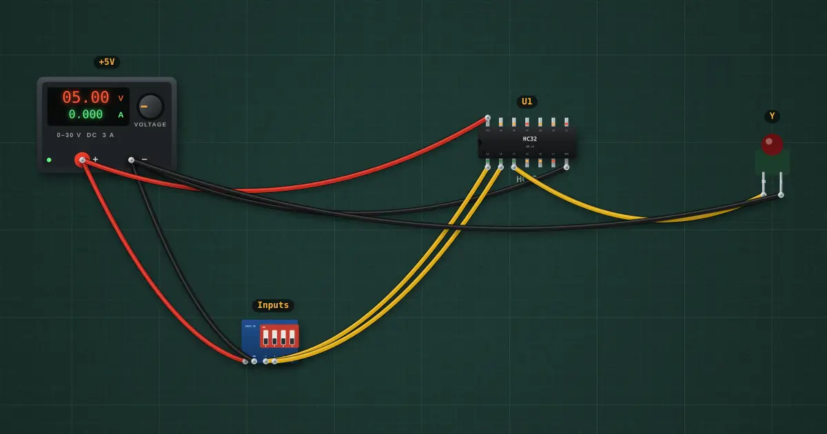
Open this lesson in the labFree, in your browser, no account needed.
How it works
Y = A + B
| A | B | Y | bench | |
|---|---|---|---|---|
| 0 | 0 | 0 | — | |
| 0 | 1 | 1 | — | |
| 1 | 0 | 1 | — | |
| 1 | 1 | 1 | — |
Flip the switches to try every row. “bench” fills in with what the chip actually did.
74HC32: quad 2-input or in one 14-pin chip. Pin 14 is +5 V, pin 7 is ground. Every unused input should be tied to VCC or GND in a real build.
Try it on the bench
- Click switches 1 and 2 to step through 00, 01, 10 and 11. Each combination fills a row of the table.
- Select U1 and change its family to 74LS: the high output drops to about 3.5 V, because TTL outputs cannot pull all the way to VCC.
- Delete the wire to input B. A floating CMOS input is undefined: the output flickers. Switch the chip to 74LS and the floating input reads as 1.
Parts on the bench
- Bench power supply
- DIP switch module
- 74xx32
- Logic indicator LED
In the course
Zen’s Electronics Design Mastery, module “Digital Electronics”.