How a PCB works: the layer stack-up
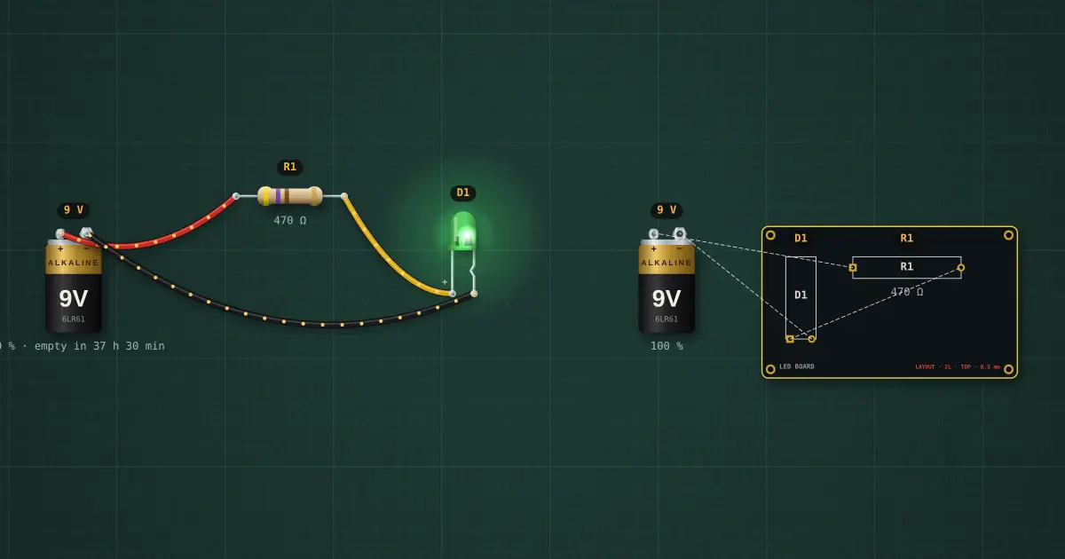
A printed circuit board is a stack: copper etched into traces and pads, glued to fibreglass, coated with solder mask and printed with labels, with plated holes joining the layers. The 3D board explorer opens over the mat: orbit it, explode it, click every layer, watch it being made, cut it in half, then take the quiz. The bench holds the same LED circuit as a schematic and as a board you can route.
Open this lesson in the labFree, in your browser, no account needed.
How it works
Explore: drag to orbit, scroll to zoom, Explode / Assemble the stack, click a layer or a pin, switch 2-layer / 4-layer, and turn on the signal and its return current.
How it is made: laminate, drill, plate, etch, mask, finish, silkscreen and assembly, step by step on the same board.
Cross-section: a cut through a through-hole pad, a via, an SMD pad and (on 4 layers) blind and buried vias, with every thickness, plus the IPC-2221 trace-width calculator.
On the bench: the board on the right was made from the circuit on the left (Tools → Lay out on a PCB). Route it along the dashed lines and compare the two LEDs.
Try it on the bench
- Explode the 4-layer stack and find the two planes.
- Use the calculator: how wide must a 3 A trace be on 1 oz copper for a 10 °C rise?
- Route the LED board on the bench: both LEDs then carry the same current.
Parts on the bench
- 2 × 9 V battery
- 2 × Resistor
- 2 × LED
- Printed circuit board
In the course
Zen’s Electronics Design Mastery, module “Fabrication — Perfboard & PCB”.