Printed circuit board
2-layer FR-4 board 102 × 66 mm · 1.6 mm · 1 oz copper · 0 nets from the schematic · showing the layout
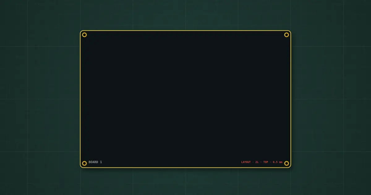
Try it on the benchThe lab drops it on an empty bench and opens its datasheet card.
Typical part: FR-4 printed circuit board, 1.6 mm, 1 oz copper, HASL finish
Pins
pads come from the parts placed on it
Ratings and limits
| Layers | 2 |
|---|---|
| Copper | 1 oz (35 µm) |
| Min. clearance (this lab) | 0.2 mm |
| Through-hole pad | 1.8 mm, 0.9 mm drill |
| Trace current (IPC-2221, +10 °C, outer) | 0.25 mm 0.9 A · 0.3 mm 1.0 A · 0.4 mm 1.2 A · 0.5 mm 1.4 A · 0.8 mm 2.0 A · 1 mm 2.4 A · 1.5 mm 3.2 A |
How to use it
Make one from a circuit with Tools → Lay out on a PCB. Drag pad to pad to route a trace on the active layer; through-hole pads and vias join the layers. The dashed ratsnest shows what is left to route; the design-rule check lists shorts, clearance and width problems.