Logic levels and families
A logic input decides 1 or 0 by comparing its voltage with two thresholds. Mixing supply voltages can land a signal in the forbidden band between them. A 3.3 V output is too low for a 5 V 74HC input (it needs 3.5 V) but fine for a 74HCT, which has TTL thresholds. Going down from 5 V, a divider protects the 3.3 V input.
Open this lesson in the labFree, in your browser, no account needed.
How it works
| family | VIL max | VIH min | VOH |
|---|---|---|---|
| 74HC at 5 V | 1.5 V | 3.5 V | ≈ 4.9 V |
| 74HCT at 5 V | 0.8 V | 2.0 V | ≈ 4.9 V |
| 74LS (TTL) | 0.8 V | 2.0 V | ≈ 3.4 V |
| 74HC at 3.3 V | 1.0 V | 2.3 V | ≈ 3.2 V |
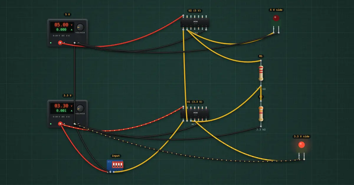
U1 runs on 3.3 V, so its high is about 3.2 V. U2 (now 74HC · CMOS) needs at least 3.5 V to see a 1.
Back down: R1 and R2 divide U2’s 5 V output to 5 × 3.3 / 5.5 = 3.0 V, safe for U1’s 3.3 V input, which needs 2.3 V. Without them, 5 V would push current through U1’s input protection diodes into its 3.3 V rail.
Try it on the bench
- With the input switch off, U1 outputs 3.2 V and U2 (74HC) flickers: 3.2 V is in its forbidden band.
- Select U2 and change its family to 74HCT: the same 3.2 V is now a solid 1. This is why 74HCT chips are used as level shifters.
- Delete R2: the 3.3 V chip now gets the full 5 V on its input, beyond its supply. Real chips survive that only through their clamp diodes, if at all.
Parts on the bench
- 2 × Bench power supply
- DIP switch module
- 2 × 74xx04
- 2 × Logic indicator LED
- 2 × Resistor
In the course
Zen’s Electronics Design Mastery, module “Digital Electronics”.