65 W USB-C PD stage on a ready-made 24 V supply: buck converter, PD controller, load switch
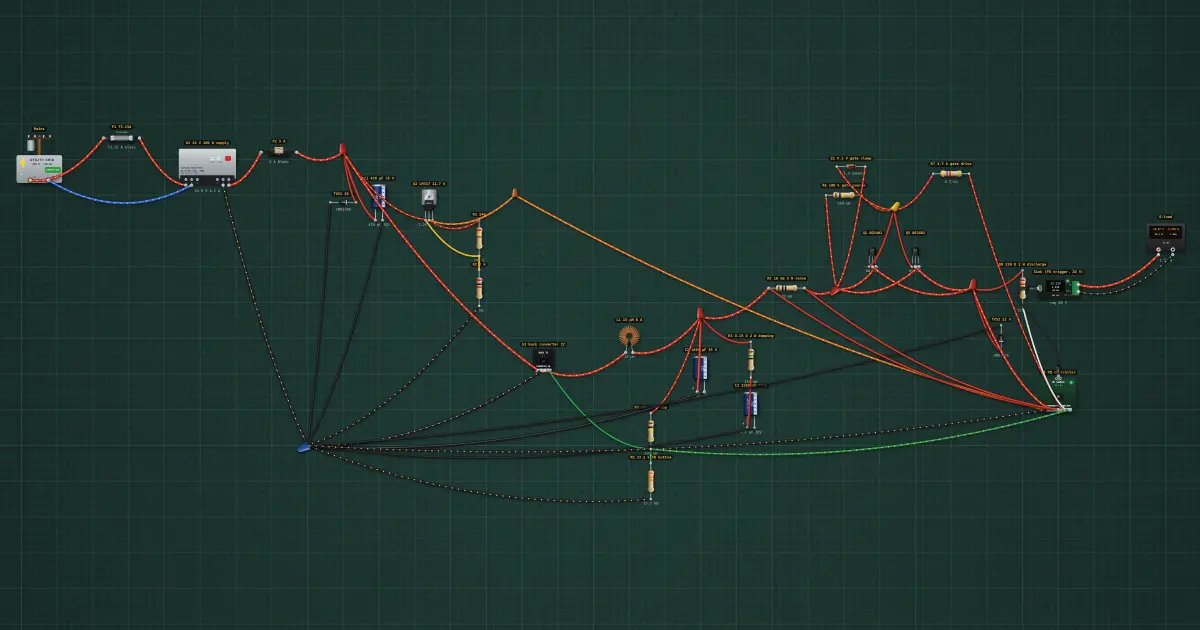
65 W USB-C PD charger: certified 24 V supply, buck converter, PD source controller, P-MOSFET load switch, with OCP, OVP, UVP and VBUS discharge. A 65 W USB-C Power Delivery charger, with the safety line drawn where a careful builder draws it. Mains to an isolated 24 V is a certified, enclosed 100 W switching supply (U1): it has its own fuse, inrush limiter, isolation transformer and Y-capacitor, and its isolation is what keeps the USB side safe to touch. This version keeps mains inside a certified supply, the quick and safe way to a bench PD source; the full build from mains up (offline flyback, opto feedback, with its safety notes) is the “65 W USB-C PD charger from scratch” build. F1 on mains L is a T3.15A slow-blow, the same rating as the fuse inside this class of supply: every time mains comes on, U1’s bulk capacitor charges through its NTC limiter (about 60 A for half a millisecond from cold, about 3× the I²t if the supply was just running and the NTC is still hot). That pulse uses about 15 % of a T3.15A’s melting I²t, but over a third of a T2A’s, and fuses that see more than about a quarter of their I²t at every switch-on age and blow after a few quick off/on cycles. Everything after the 24 V is built from parts, and every node can be metered. Input: F2 (5 A) and TVS1 (28 V) protect the 24 V rail; C1 470 µF 35 V is the converter’s input reservoir; U2, an LM317 at 11.7 V, powers the PD controller. Converter: U3 is a synchronous buck IC (36 V, 8 A, FB 1.25 V; the bench models it averaged, the switch node as duty × VIN) with L1 15 µH, C2 1000 µF and a damping branch R3 0.15 Ω + C3 2200 µF, all rated 35 V: if the feedback ever breaks, this buck can drive its output to 95 % of 24 V, and a 25 V capacitor would sit at its limit (low-ESR output capacitors with an inductor ring; the damping branch kills it). R4 100 k / R5 33.2 k set 5.0 V. Output: RS 10 mΩ senses the current (Kelvin-connected: ISP and ISN go to the resistor’s own ends, so the drop in the power wires is not read as current); Q2 and Q3, two AO3401 P-MOSFETs in parallel, are the load switch (each carries half, well inside its 4 A); Z1 9.1 V clamps their gate so they never see more than −9 V, R6 holds them off, R7 is the gate drive. TVS2 22 V and R8 220 Ω discharge sit on VBUS. U4, the PD controller: Rp on CC, attach debounce, it closes the load switch only when the converter is at 4.75–5.5 V (vSafe5V), sends Source_Capabilities (5, 9, 15 V at 3 A, 20 V at 3.25 A only on a 5 A cable, otherwise 20 V 3 A), raises the output by sinking current from FB through R4 (Vout = 5 V + I × 100 kΩ), signals PS_RDY when VOUT is within 5 %, and protects: over-current 115 % for 10 ms (6 A at once), over-voltage 115 % (latched until unplugged), under-voltage (a short) for 50 ms, VBUS discharged to 0 V on unplug. Meter it: mains watts, 24 V and its current, VOUT, the drop across RS (33 mV at 3.3 A), the gate-source voltage of Q2/Q3, VBUS at the port and at the sink (the cable drops about 0.6 V at 3.3 A on 1 m of 20 AWG), and the controller’s PD log.
Build it in the labGuided build, test sheet and fault finding, free in your browser.
Parts list
- Utility grid
- 2 × Fuse
- Switching power supply
- 2 × TVS diode
- 3 × Electrolytic capacitor
- LM317 / LM338 regulator
- 9 × Resistor
- Synchronous buck converter IC
- Toroidal inductor
- 2 × P-channel MOSFET
- Zener diode
- USB-C PD source controller
- USB-C PD trigger + meter
- Electronic load
Test procedure
Each test has an expected value and a pass range, like a factory test sheet:
- 5 V on a plain Type-C sink (no PD)
- PD 20 V contract on a 5 A cable
- …and it delivers 65 W
- A 3 A cable only gets 20 V 3 A
- PD 9 V contract (a phone-like sink)
- Overload: 4.5 A on a 3.25 A contract trips the load switch
- Short on VBUS: the controller cuts it, nothing burns
- FB top resistor open: the converter runs away, the sink is never connected
- Unplugged: VBUS is discharged to vSafe0V
- Mains off and on three times at full load: F1 survives
- …and the charger comes back to 20 V by itself
- The 24 V supply runs inside its rating at full load
- Each load-switch MOSFET carries half
How it works
What it does: 65 W USB-C PD charger: certified 24 V supply, buck converter, PD source controller, P-MOSFET load switch, with OCP, OVP, UVP and VBUS discharge.
Build it (guided or ready-made), then run its test procedure below. Every test has an expected value and a pass range, just like a factory test sheet.
Background
Small GaN chargers do all of this in one box: an offline flyback whose secondary is set by a PD controller through the same FB-current trick, the load switch and the discharge. Bench-built PD supplies split it the way this one does: a certified mains supply, then a PD buck stage.