65 W USB-C PD charger from scratch: mains flyback (UC3844, 800 V MOSFET, PQ2625 transformer), TL431 + PC817 feedback, PD controller
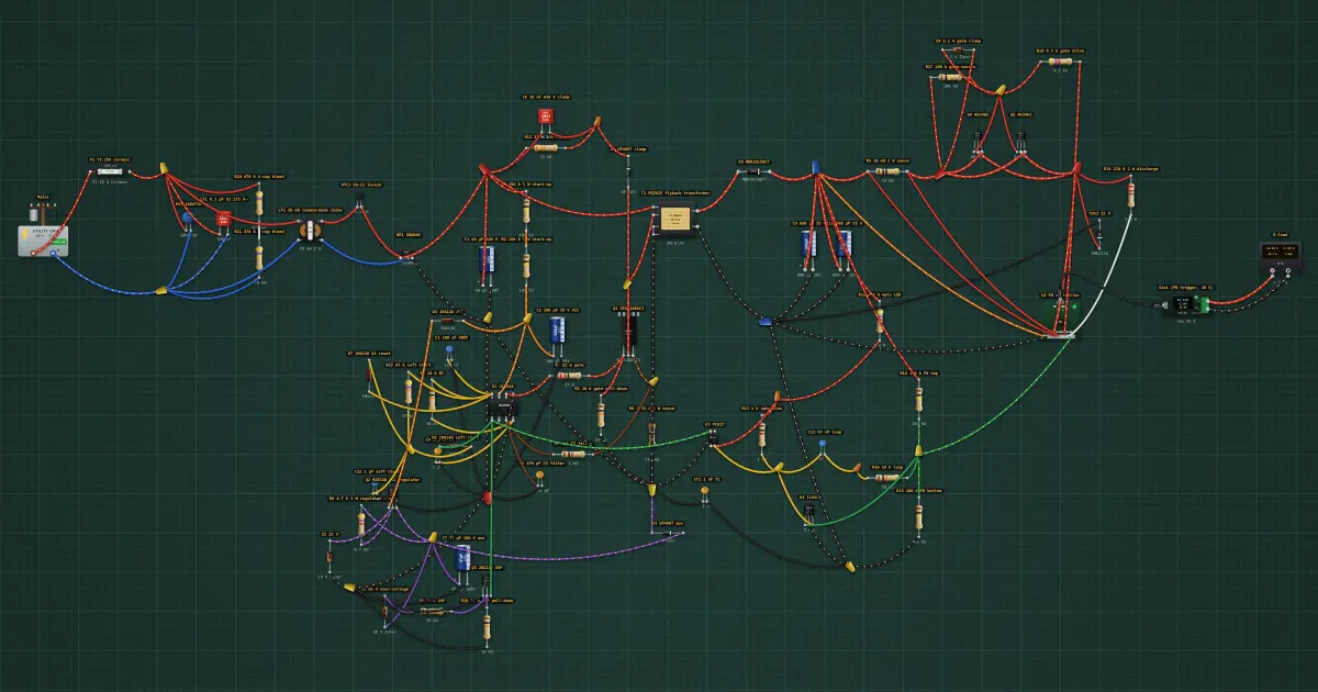
65 W USB-C PD charger from parts: mains input filter, bridge and bulk, UC3844 flyback with RCD clamp and aux-powered VCC, TL431 + PC817 feedback, primary OVP, PD controller and load switch. A 65 W USB-C PD charger built from parts, mains to plug: the same architecture as a commercial charger, an offline flyback with an opto-isolated feedback loop and a PD controller on the secondary. READ THIS BEFORE BUILDING IT FOR REAL. Everything on the primary side (left of T1 and the optocoupler) is at mains potential: C1 charges to about 311 V DC at 220 V and stays charged after you unplug (it bleeds through R1/R2, about a minute to fall below 50 V; measure before you touch). Power the board for the first time through a 1:1 isolation transformer and a series 60–100 W incandescent lamp (dim-bulb tester), with a CAT II or better meter, one hand on the bench, and never clip a mains-earthed scope to the primary. Keep 6.4 mm or more of creepage between anything primary and anything secondary on the board (a routed slot under T1 and U3), use triple-insulated wire for the secondary winding, and use only a Y1-rated capacitor for CY1. A charger built at home has no safety certification; use it on the bench, not in a child’s room. Input: F1 T3.15A ceramic (sand-filled: a short behind the bridge can draw far more than the 35 A a glass tube can break), RV1 14D471K against surges, CX1 0.1 µF X2 with R20/R21 to discharge it when unplugged, LF1 common-mode choke (conducted EMI), NTC1 5D-11 to limit the inrush into C1 (about 57 A for a fraction of a millisecond, the bridge GBU806 takes 200 A), C1 68 µF 400 V (about 1 µF per watt at 220 V; 30 V of 120 Hz ripple at full load). Primary: U1 UC3844, current mode, RT 10 k / CT 1.2 nF → 143 kHz oscillator, 72 kHz at the gate, 48 % maximum duty. R6 0.33 Ω sets the cycle-by-cycle limit at 1 V / 0.33 Ω = 3.0 A, under T1’s 3.4 A saturation. Q1 SPA11N80C3 (800 V CoolMOS, insulated tab, on a heatsink). T1 PQ26/25: Np 40, Ns 8 (V_OR about 104 V at 20 V out), Na 22, Lp 450 µH, about 4 µH leakage. D2 / C8 / R11 clamp the leakage spike to about 200 V above the bulk, so the drain peaks near 520 V at 220 V mains (65 % of 800 V). Start-up: R1 + R2 (200 k, ½ W each) charge C2 (100 µF) until VCC reaches 16 V (about 1.5 s); R22 / C12 / D6 then let COMP rise over a few tens of milliseconds (soft start: no full-power slam into the empty output capacitors), and D7 resets C12 whenever VREF drops. C2 has to carry the controller for those milliseconds until the aux winding takes over: (Na/Ns) × (VOUT + 0.5 V) is about 15 V at 5 V out and 56 V at 20 V out, so Q2 MJE340 with Z2 15 V holds VCC near 13 V across the whole PD range (R8 is a 1 W part: it drops 41 V at 20 V out), and D4 stops C2 from back-feeding Q2. Over-voltage: if the secondary loop ever fails, the aux rail climbs with VOUT; at about 69 V (VOUT ≈ 24.5 V) Z3 (68 V) conducts, Q3 pulls COMP down and holds the output there, under the 35 V caps and the PD controller’s 24 V limit. Secondary: D5 MBR20150CT (150 V, the reverse peak is VOUT + bulk ÷ 5, about 85 V), C9 + C10 680 µF 35 V (use low-ESR or solid polymer: the ripple current is several amps). U4 TL431 with R14/R15 100 k / 100 k regulates 5.0 V; R12 feeds the opto LED from VOUT, R13 keeps the TL431 biased, C11 + R16 compensate the loop. U2, the PD controller, raises VOUT by sinking current from the TL431 REF node (VOUT = 5 V + I × 100 k), then the same load switch, sense and discharge as any PD source. Meter it: mains current (it is peaky: rms is about twice the average), C1’s voltage, VCC during start-up and running, COMP (around 2–4 V), the average drain voltage (equals the bulk on a DC meter), D5’s drop, VOUT at each PD level, the aux rail (15 → 56 V as VOUT goes 5 → 20 V). The switching itself is averaged in this simulator: peaks (drain voltage, diode reverse, primary peak current) are in T1’s and Q1’s readings.
Build it in the labGuided build, test sheet and fault finding, free in your browser.
Parts list
- Utility grid
- Fuse
- MOV varistor
- 2 × Film capacitor
- 23 × Resistor
- Common-mode choke
- NTC thermistor
- Bridge rectifier
- 5 × Electrolytic capacitor
- Flyback transformer
- 2 × Rectifier diode
- High-voltage N-MOSFET
- Current-mode PWM controller
- 6 × Ceramic capacitor
- 3 × Signal diode
- NPN transistor, 300 V
- 3 × Zener diode
- NPN transistor
- Schottky diode
- Optocoupler
- TL431 reference
- 2 × P-channel MOSFET
- TVS diode
- USB-C PD source controller
- USB-C PD trigger + meter
- Electronic load
Test procedure
Each test has an expected value and a pass range, like a factory test sheet:
- C1 charges to the mains peak
- UC3844 starts from R1 + R2 and the aux winding takes over
- 5 V on a plain Type-C sink (no PD)
- PD 9 V contract (a phone-like sink)
- PD 20 V on a 5 A cable, 65 W
- Efficiency at 65 W, mains to port
- Q1 drain peak at full load
- D5 reverse peak at full load
- T1 stays out of saturation at full load
- VCC stays regulated at 20 V out
- Short on VOUT: hiccup, nothing burns
- Opto LED open: the primary OVP holds VOUT, the PD switch opens
- Mains off and on three times at full load: F1 survives
How it works
What it does: 65 W USB-C PD charger from parts: mains input filter, bridge and bulk, UC3844 flyback with RCD clamp and aux-powered VCC, TL431 + PC817 feedback, primary OVP, PD controller and load switch.
Build it (guided or ready-made), then run its test procedure below. Every test has an expected value and a pass range, just like a factory test sheet.
Background
This is the shape of almost every USB-C charger: a flyback (quasi-resonant in the newest, with GaN switches at 100–200 kHz, which is how they shrink) and a secondary PD controller that moves the output by pulling on the feedback node. The UC3842/3/4/5 family (1984) is still in thousands of supplies and is the classic part to build one from.