Real device: phone charger, 220 V AC wall to 5 V USB
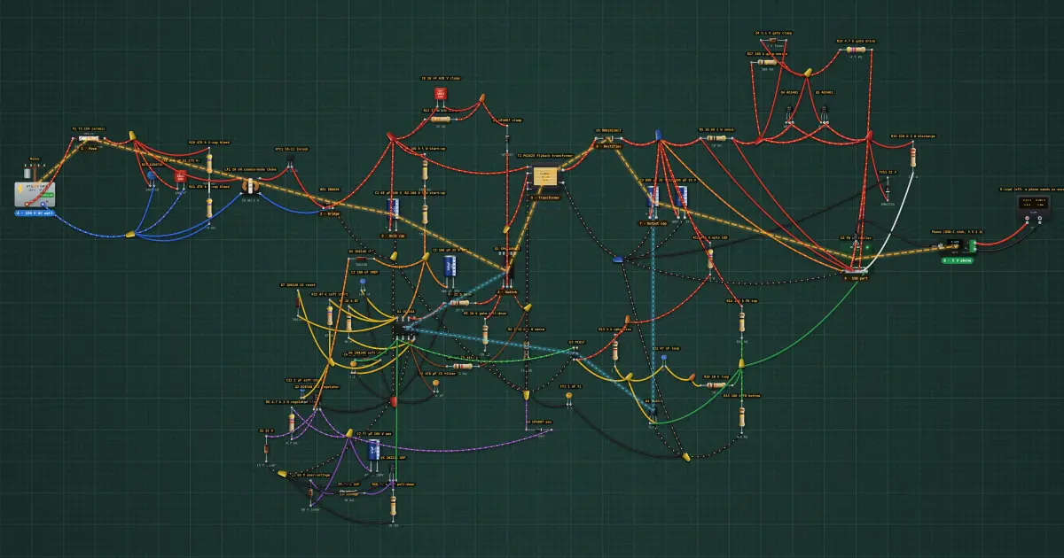
A USB phone charger traced from the wall to the phone, every part annotated: fuse, bridge, bulk capacitor, switching transformer, opto feedback, output capacitor.
Build it in the labGuided build, test sheet and fault finding, free in your browser.
Parts list
- Utility grid
- Fuse
- MOV varistor
- 2 × Film capacitor
- 23 × Resistor
- Common-mode choke
- NTC thermistor
- Bridge rectifier
- 5 × Electrolytic capacitor
- Flyback transformer
- 2 × Rectifier diode
- High-voltage N-MOSFET
- Current-mode PWM controller
- 6 × Ceramic capacitor
- 3 × Signal diode
- NPN transistor, 300 V
- 3 × Zener diode
- NPN transistor
- Schottky diode
- Optocoupler
- TL431 reference
- 2 × P-channel MOSFET
- TVS diode
- USB-C PD source controller
- USB-C PD trigger + meter
- Electronic load
Test procedure
Each test has an expected value and a pass range, like a factory test sheet:
- C1 charges to the mains peak
- 5 V at the phone
- 2 A into the phone
- Output isolated: the only paths across are T1, U3 and CY1
How it works
Every phone charger sold for the last fifteen years is the same machine: rectify the mains, chop it at tens of kilohertz into a small transformer, and use light to tell the primary how the output is doing. This one is the lab's 65 W USB-C charger delivering 5 V to a phone; a 10–20 W charger has exactly these blocks, just a smaller transformer and capacitors.
A220 V AC at the wall plug.BA regulated 5 V on the USB port, isolated from the mains.
The path, A to B
- 220 V AC wall (Mains). Point A: the wall, 220 V at 60 Hz, which peaks at 311 V. Everything on the left of the transformer and the optocoupler is at this potential.
- Fuse (F1). Fault safety. A slow-blow 3.15 A fuse that ignores the switch-on surge but opens if anything behind it shorts, so a failed part becomes a dead charger instead of a fire. Ceramic and sand-filled, because a short right behind the bridge can draw far more current than a glass tube can safely break.
- Bridge (BR1). AC to pulsing DC. Four diodes flip the negative half of every cycle up, giving 120 bumps a second that all point the same way.
- Bulk cap (C1). Smoothing. A 68 µF 400 V electrolytic fills in between the bumps, so the switcher sees a steady ~300 V DC with a little 120 Hz ripple. It is also the part that stays charged after unplugging.
- Switch (Q1). The switch. An 800 V MOSFET chops the bulk voltage into the transformer about 70,000 times a second. Switching that fast is what lets a transformer the size of a sugar cube do the work of a 60 Hz one ten times its weight.
- Transformer (T1). Step-down and isolation in one. The flyback transformer stores energy in its core while Q1 is on and hands it to the secondary when Q1 turns off. The 40 : 8 turns ratio brings ~300 V down to the output, and the insulation between the windings is what keeps the mains away from you.
- Rectifier (D5). Output rectifier. A dual Schottky: its low forward drop means less heat at several amps.
- Output cap (C9). Clean output. With C10, 1360 µF of low-ESR capacitance soaks up the transformer's pulses and leaves steady DC. Two in parallel share the ripple current, which is what wears electrolytics out.
- USB port (U2). The PD controller. It talks to the device over the cable's CC wire, agrees a voltage, then moves the output there by pulling on the TL431's divider.
- 5 V phone (Phone). Point B: the phone. It asks for nothing more than 5 V, so the PD controller never moves the output from the TL431's base 5.0 V. 2 A here is 10 W.
The loop back: C9 → U4 (TL431) → U3 (opto) → U1 → Q1. If the output rises, the TL431 brightens the opto's LED, U1 ends each pulse sooner and less energy goes through T1. This loop is the regulation, and it crosses the isolation gap as light.
Every other part, and why
- RV1: Surge clamp. A varistor that conducts hard above about 470 V peak, soaking up lightning and switching spikes on the line before they reach the bridge and the MOSFET.
- CX1: Noise filter. An X2 safety capacitor across the line shorts the charger's own high-frequency noise back on itself so it doesn't travel down the house wiring. X2-rated means it is built to fail open, never short.
- R20: Safety bleed. With R21 it drains CX1 after you pull the plug, so the pins can't bite you. Two in series because one small resistor isn't rated for the whole mains voltage.
- R21: Safety bleed, the second half of R20 (see R20).
- LF1: Noise filter. A common-mode choke: line and neutral are wound on one core, so the normal 60 Hz current cancels in it, while noise that leaves on both wires together sees a high impedance.
- NTC1: Inrush limiter. Cold, it is about 5 Ω, which tames the surge into the empty C1 at switch-on. Current warms it and it drops to a fraction of an ohm, so it costs almost nothing while running.
- U1: The primary-side brain. The UC3844 runs the oscillator, drives Q1's gate, and ends each pulse when the current in R6 reaches the level the feedback asks for.
- R6: Current sense. The voltage across 0.33 Ω tells U1 the transformer current on every cycle; at 1 V (3 A) U1 cuts the pulse short. That is the built-in short-circuit limit, acting within microseconds.
- D2: Clamp. Each time Q1 turns off, the transformer's leakage inductance kicks a spike. D2 dumps it into C8, and R11 burns it off as heat, so the drain stays well under 800 V.
- C8: Clamp capacitor: catches the leakage spike (see D2).
- R11: Clamp resistor: turns the caught spike into heat (see D2). 3 W because it does this 70,000 times a second.
- R1: Start-up. Before the transformer runs there is no aux power, so R1 and R2 trickle current from the bulk into C2 until U1 has enough voltage to start.
- R2: Start-up, with R1. Two in series to share the voltage.
- C2: VCC store. Holds U1's supply up during start-up and between aux pulses.
- C3: Decoupling for U1's 5 V reference, so the timing and the current limit stay clean.
- R3: Timing, with C4: sets U1's oscillator at about 143 kHz, 72 kHz at the gate.
- C4: Timing capacitor (see R3).
- R22: Soft start, with C12: lets the output come up over tens of milliseconds instead of slamming the transformer at full power.
- C12: Soft-start capacitor (see R22).
- D6: Soft-start diode: holds COMP down while C12 charges.
- D7: Resets the soft start when the controller stops, so every restart is soft too.
- R4: Gate resistor: slows Q1's edges slightly, cutting ringing and radio noise.
- R5: Gate pull-down: keeps Q1 firmly off whenever U1 isn't driving it, so it can never sit half-on and cook.
- R7: Current-sense filter, with C6: hides the spike at the start of each pulse so U1 doesn't mistake it for an overcurrent.
- C6: Current-sense filter capacitor (see R7).
- D3: Aux supply. A small extra winding on T1 powers U1 once switching starts, so the start-up resistors only work for a second.
- C7: Aux reservoir for the winding's pulses.
- Q2: VCC regulator. The aux voltage rises with the output (5 V → 20 V); Q2 with R8 and Z2 holds U1's VCC near 14 V either way.
- R8: Bias for the VCC regulator (see Q2).
- Z2: 15 V reference for the VCC regulator (see Q2).
- D4: Steers the regulated aux into VCC.
- Z3: Over-voltage watch, the second way to stop. If the feedback fails and the output soars, the aux rises with it; Z3 conducts, Q3 pulls COMP down and U1 stops switching.
- R9: Over-voltage network (see Z3).
- R10: Over-voltage network (see Z3).
- Q3: Over-voltage switch (see Z3).
- C10: Output capacitor, sharing the ripple with C9.
- CY1: Y capacitor. Gives high-frequency noise a short way back to the primary instead of out along your cable. Y-rated, so it fails open: it bridges the isolation barrier.
- U3: Regulation across the barrier. The opto's LED on the output side tells the primary how hard to work, with light, so no wire crosses the isolation gap.
- R12: Feeds the opto LED from the output.
- R13: Keeps the TL431 biased even when the opto LED is nearly off.
- U4: The reference. The TL431 compares the output (through R14 and R15) with its own precise 2.5 V and pulls more current through the opto LED as the output rises.
- R14: Output divider top: with R15, 2.5 V at the TL431 means 5.0 V out.
- R15: Output divider bottom (see R14).
- C11: Loop compensation, with R16: sets how fast the loop reacts so it settles instead of oscillating.
- R16: Loop compensation (see C11).
- RS: USB current sense: the PD controller reads it to hold the current it agreed with the device.
- Q4: Load switch, with Q5. Back-to-back P-MOSFETs keep the port dead until a device asks for power, and stop current flowing back in.
- Q5: Load switch, the second half of the back-to-back pair (see Q4).
- R17: Gate pull-up: holds the load switch off by default.
- Z4: Gate clamp: keeps the load switch's gate under its 12 V limit at 20 V out.
- R18: Gate drive from the PD controller.
- TVS1: Clamps spikes on the port, from hot-plugging or a static zap.
- R19: Discharge: pulls the port down fast when the voltage steps down or the cable is unplugged.
- E-load: Switched off here: a phone needs only the 2 A the USB sink draws. The laptop build turns it on.
Why it lasts
- Isolation by construction. Only three things cross from the mains side to the output: the transformer's insulated windings, the opto's light gap and one Y-rated capacitor, with at least 6 mm of creepage around them. A fault on the primary side cannot reach the USB pins.
- Margins on every stressed part: Q1 sees about 520 V of its 800 V, D5 about 85 V of 150 V, C1 311 V of 400 V, and T1's peak flux stays under 85 % of saturation even at 65 W. At 10 W for a phone, every part is loafing.
- More than one way to stop. Cycle-by-cycle current limit in R6, the opto feedback loop, the separate over-voltage watch (Z3/Q3) and finally the fuse. Any one of them failing still leaves the others.
- Gentle starts. NTC1 and the soft start mean every plug-in is a small event instead of a slam, every day for years.
- What wears out is heat: electrolytic capacitors lose about half their life for every 10 °C hotter they run. Turn on the Thermal view: the hot parts are Q1, T1 and D5, and the output capacitors sit away from them on purpose.
On the mat: the amber line is the energy path from A to B, the dashed blue line the feedback loop. Click any part: why it is there shows at the top of the inspector. Turn the path off or on in the View menu (Real-device path & notes); the Thermal view shows where the heat goes.
Background
The offline flyback with a TL431 and an optocoupler became the standard small power supply in the late 1980s, and the UC384x controller (1984) is still in thousands of products. Newer chargers add GaN switches and quasi-resonant timing to shrink, but the path from A to B is the same.